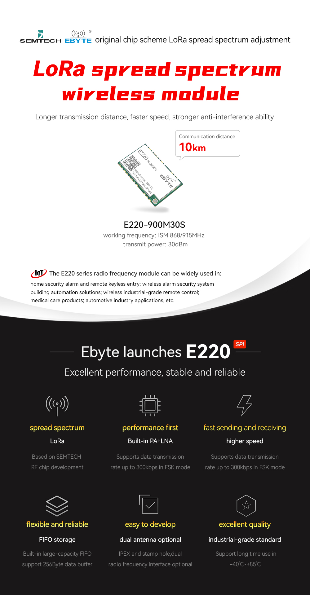
E220-M Series, LoRa Spread Spectrum Wireless Module E220-900M30S
E220-900M30S
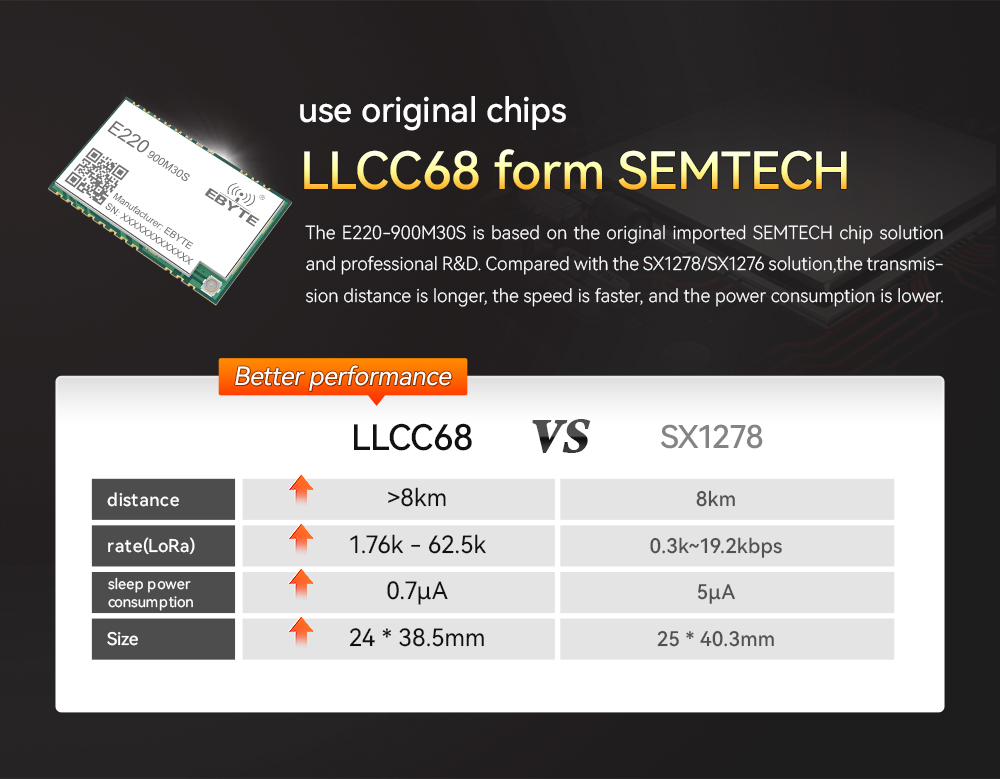
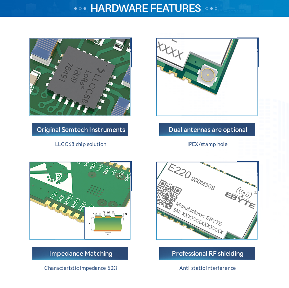
[IC]:LLCC68
[Frequency]:850.125~930.125MHz
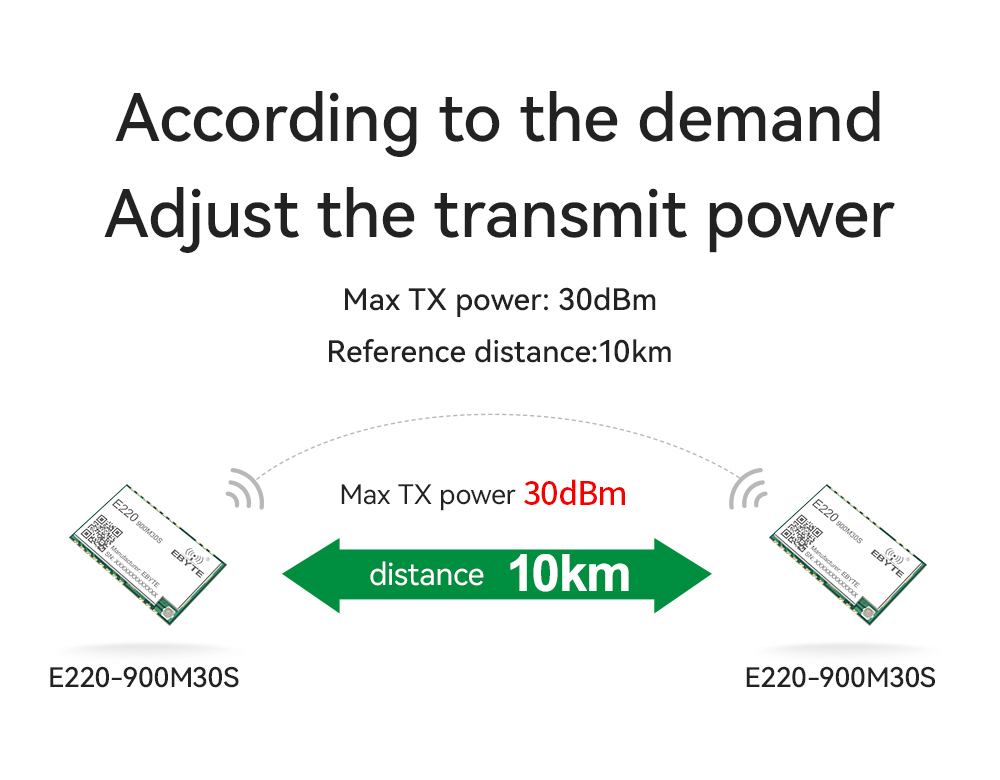
[Power]:30dBm
[Distance]:10km
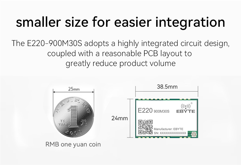
[Size]:38.5*24mm
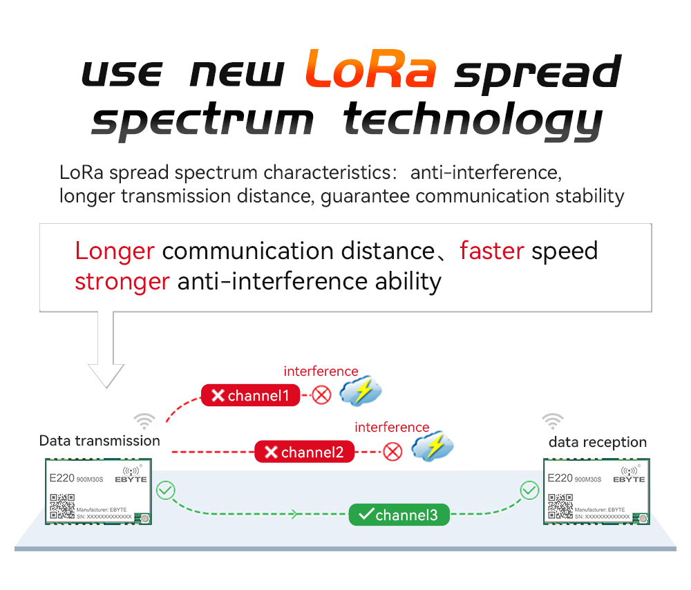
[Introduction]:E220-900M30S is 1W module developed independently based on new generation of LoRa RF chip LLCC68 from Semtech. LLCC68 is suitable for 868MHz/915MHz SMD wireless module and uses industrial 32mhz crystal oscillator.
| Model | Communication interface | IC | Frequency(Hz) | Tx power(dBm) | Distance(km) | Air data | Package | Size(mm) | Feature | Manual |
| E220-400M22S | SPI | LLCC68 | 433M 470M | 22 | 6 | 1.76~62.5k/0.6~300k | SMD | 20*14*2.8 | New generation LoRa modulation technology | ✔ |
| E220-400M30S | SPI | LLCC68 | 433M 470M | 30 | 10 | 1.76~62.5k/0.6~300k | SMD | 38.5*24 | New generation of LoRa spread spectrum technology | ✔ |
| E220-900M30S | SPI | LLCC68 | 868M 915M | 30 | 10 | 1.76~62.5k/0.6~300k | SMD | 38.5*24 | New generation of LoRa spread spectrum technology | ✔ |
| E220-900M22S | SPI | LLCC68 | 868M 915M | 22 | 6 | 1.76~62.5k/0.6~300k | SMD | 20*14*2.8 | New generation LoRa modulation technology | ✔ |
| Main parameter | Performance |
Remarks |
| Reference distance |
10km |
In clear and open environment, the antenna gain is 5dBi, the antenna height is 2.5m, and the air speed is 2.4kbps. |
| FIFO |
256Byte |
Maximum length of single transmission |
| Crystal frequency |
32MHz |
Passive crystal oscillator, 24pF is recommended |
| Modulation mode |
LORA |
Lora modulation is recommended |
| Packaging method |
SMD |
- |
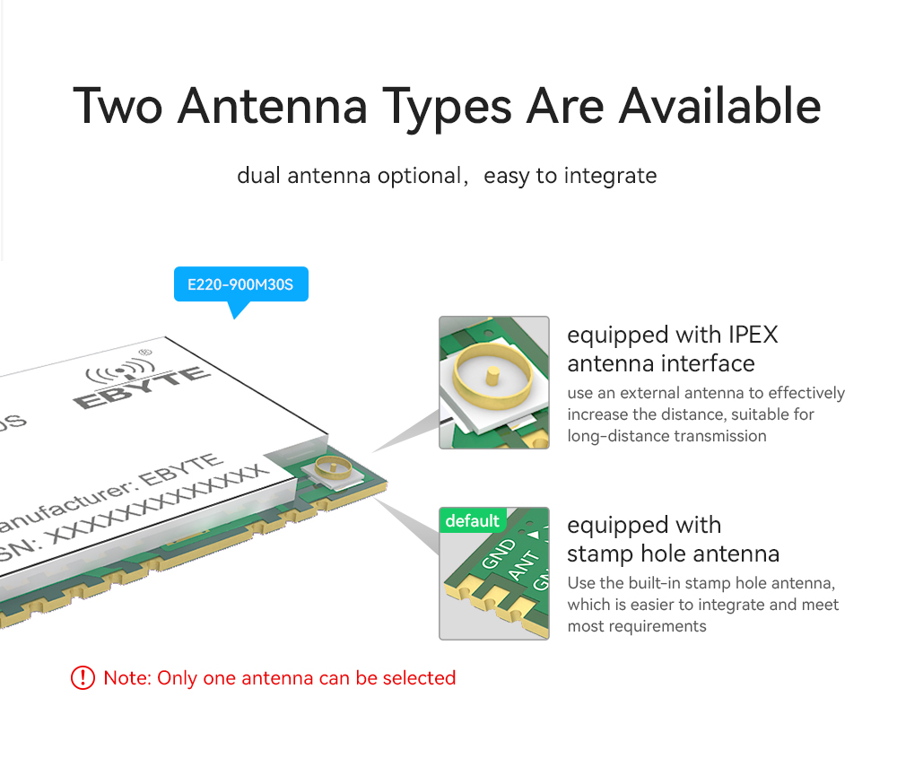
| Interface mode |
Stamp hole |
The spacing is 2.54mm |
| Communication interface |
SPI |
0~10Mbps |
| Dimension |
38.5*24mm |
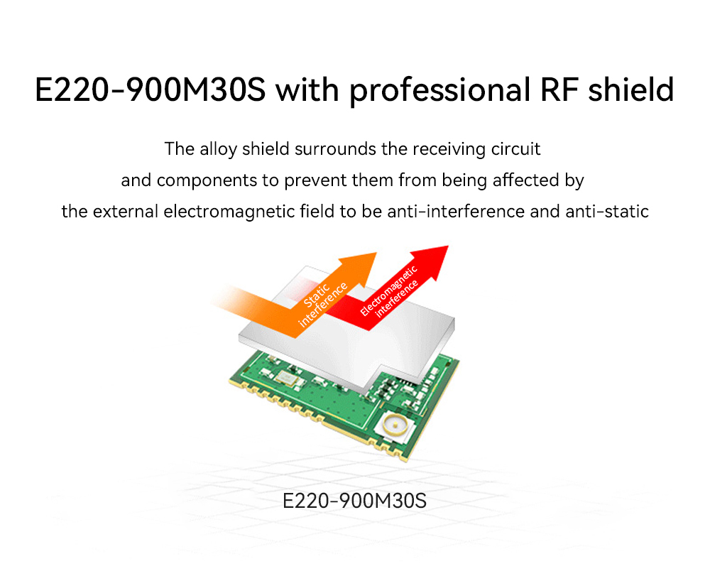
Including shield |
| RF interface |
Stamp hole / IPEX |
- |
| Main parameter | Min. | Typ. | Max. | Unit | Remarks |
| Working voltage |
3 | 5 | 5.5 | V | ≥5.5 V ensures output power |
| Operating frequency band |
850 | 868/915 |
930 |
MHz |
Support ISM band |
| Communication level | - | 3.3 | - | V | Probably burnout when using 5V TTL |
| TX current | - |
700 | - | mA | Instantaneous power consumption |
| RX current | - | 14 |
- | mA |
- |
| Sleep current | - | 0.7 |
- | μA | Software shutdown |
| Working temperature |
-40 | - |
+85 | ℃ | Industrial Design |
| Max TX power |
29.5 | 30 | 30.5 | dBm |
- |
| Receiving sensitivity |
- |
-129 |
- |
dBm |
-124dbm,BW_L=125kHz,SF = 7,LORA TM; -129dbm,BW_L=125kHz,SF = 9,LORA TM; -121dbm,BW_L=250kHz,SF = 7,LORA TM; -129dbm,BW_L=250kHz,SF = 10,LORA TM; -117dbm,BW_L=500kHz,SF = 7,LORA TM; -127dbm,BW_L=500kHz,SF = 11,LORA TM; |
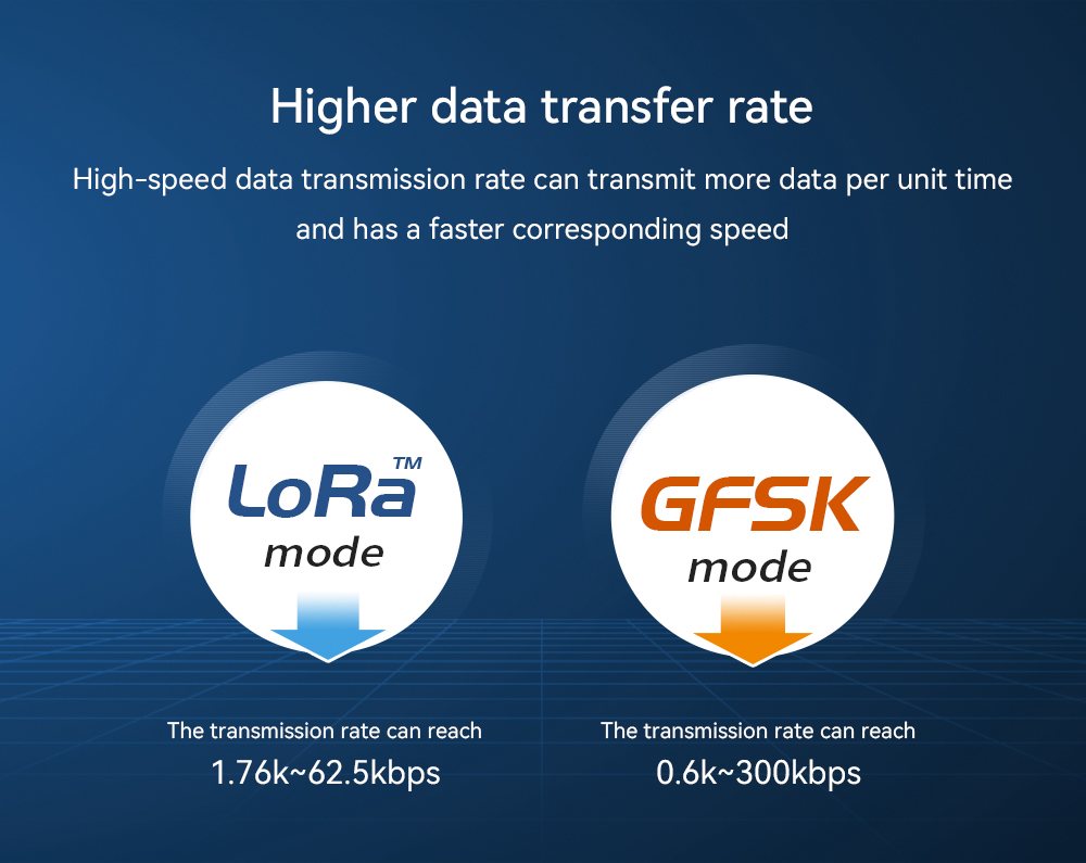
| GFSK(bps) |
0.6k | - | 300k | bps |
User programming control |
| LoRa(bps) |
1.76k | - | 62.5k | bps |
User programming control |


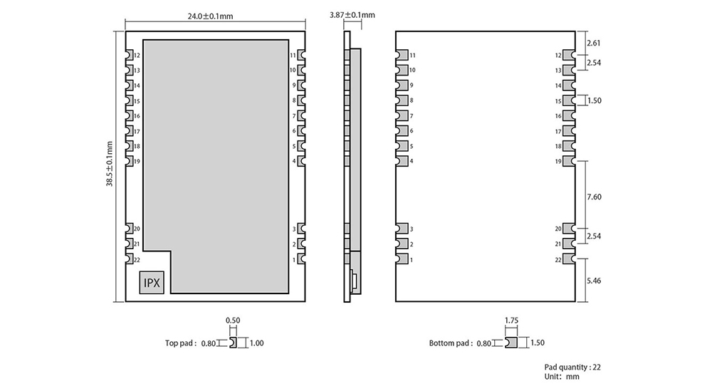
| Pin No. |
Item | Direction | Description |
| 1 | GND | - |
Ground, connect to power reference ground |
| 2 | GND | - |
Ground, connect to power reference ground |
| 3 | GND | - |
Ground, connect to power reference ground |
| 4 | GND | - |
Ground, connect to power reference ground |
| 5 | GND |
- |
Ground, connect to power reference ground |
| 6 | RXEN |
Input |
RF switch receive control pin, connect external MCU IO, high level effective |
| 7 | TXEN |
Input |
RF switch emission control pin, connected to external MCU IO or dio2,high level effective |
| 8 | DIO2 |
Input / output |
Configurable universal IO port (see llcc68 manual for details) |
| 9 | VCC |
- |
Power supply, range 3V ~ 5.5V (it is recommended to add ceramic filter capacitor externally) |
| 10 | VCC |
- | Power supply, range 3V ~ 5.5V (it is recommended to add ceramic filter capacitor externally) |
| 11 | GND | - |
Ground, connect to power reference ground |
| 12 | GND |
- |
Ground, connect to power reference ground |
| 13 | DIO1 |
Input / output |
Configurable universal IO port (see LLCC68 manual for details) |
| 14 | BUSY |
Output |
For status indication (see LLCC68 manual for details) |
| 15 | NRST |
Input |
Chip reset trigger input pin, low level effective |
| 16 | MISO |
Output |
SPI data output pin |
| 17 | MOSI |
Input |
SPI data input pin |
| 18 | SCK |
Input |
SPI data input pin |
| 19 | NSS |
Input |
The module chip selection pin is used to start a SPI communication |
| 20 | GND | - |
Ground, connect to power reference ground |
| 21 | ANT | - |
RF interface, stamp hole |
| 22 | GND | - |
Ground, connect to power reference ground |